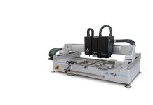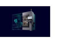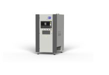
Koh Young Technology, the industry leader in True3D™ measurement-based inspection solutions, will showcase its growing portfolio of inspection and metrology technologies for semiconductor and advanced packaging applications at SEMICON West 2026, October 13–15 at the Moscone Center in San Francisco, California. Visitors to Booth 947 will see the Meister S+ for micro solder and flux inspection and the Meister D+ for advanced die inspection, while Koh Young will highlight its ZenStar for wafer-level applications.
Advanced packaging is evolving across multiple architectures rather than converging around a single manufacturing approach. System-in-package (SiP), flip-chip BGA and CSP, fan-out, panel-level packaging, wafer-level packaging, and other heterogeneous integration technologies each introduce different inspection and dimensional measurement requirements. At the same time, finer features, tighter process windows, substrate warpage, highly reflective surfaces, and increasingly complex package structures are challenging conventional optical inspection techniques.
Koh Young is addressing those challenges with a portfolio built on accurate, repeatable 3D measurement while adapting resolution, optics, algorithms, and material handling to the requirements of each process.
Meister S+ Targets Micro Solder and Flux Deposition
The Meister S+ brings high-resolution True 3D measurement to micro solder and flux deposition processes used throughout semiconductor packaging and heterogeneous integration. Designed for demanding micro-scale applications, the Meister S+ combines high-resolution optics and advanced measurement algorithms to characterize solder and flux deposits before subsequent assembly processes add additional value to the package. Its resolution supports measurement of extremely thin deposits, while specialized optical technology enables inspection of transparent flux, an application that presents significant challenges for conventional optical techniques.
The platform also addresses substrate and carrier warpage, an increasingly important consideration as package dimensions grow and structures become thinner. Enhanced warpage compensation helps maintain reliable dimensional measurement across challenging substrates and package configurations.
By providing objective 3D data on deposition conditions, the Meister S+ gives process engineers real-time visibility into variations that can influence downstream attach quality, interconnect formation, and overall package yield.
Meister D+ Measures Highly Reflective Die
Following deposition and interconnect formation, die placement introduces a different set of inspection challenges. Highly reflective and mirror-finish die surfaces can make accurate optical reconstruction difficult, particularly as die become smaller, spacing becomes tighter, and dimensional tolerances narrow.
The Meister D+ combines Koh Young’s Moiré measurement technology with proprietary optics engineered to inspect highly reflective die and package features. Its True 3D capabilities allow manufacturers to evaluate die height, tilt, coplanarity, and position while also detecting conditions such as micro-cracks, chipping, foreign material, and other defects that can compromise package integrity.
The system supports small die and narrow-gap inspection down to 50 µm, making it suitable for high-density packaging applications where conventional approaches can struggle.
Rather than simply determining whether a die is present, the Meister D+ provides dimensional information engineers can use to understand the quality of the placement process and identify variation before it propagates into subsequent manufacturing stages.
ZenStar Extends the Strategy to Wafer-Level Inspection
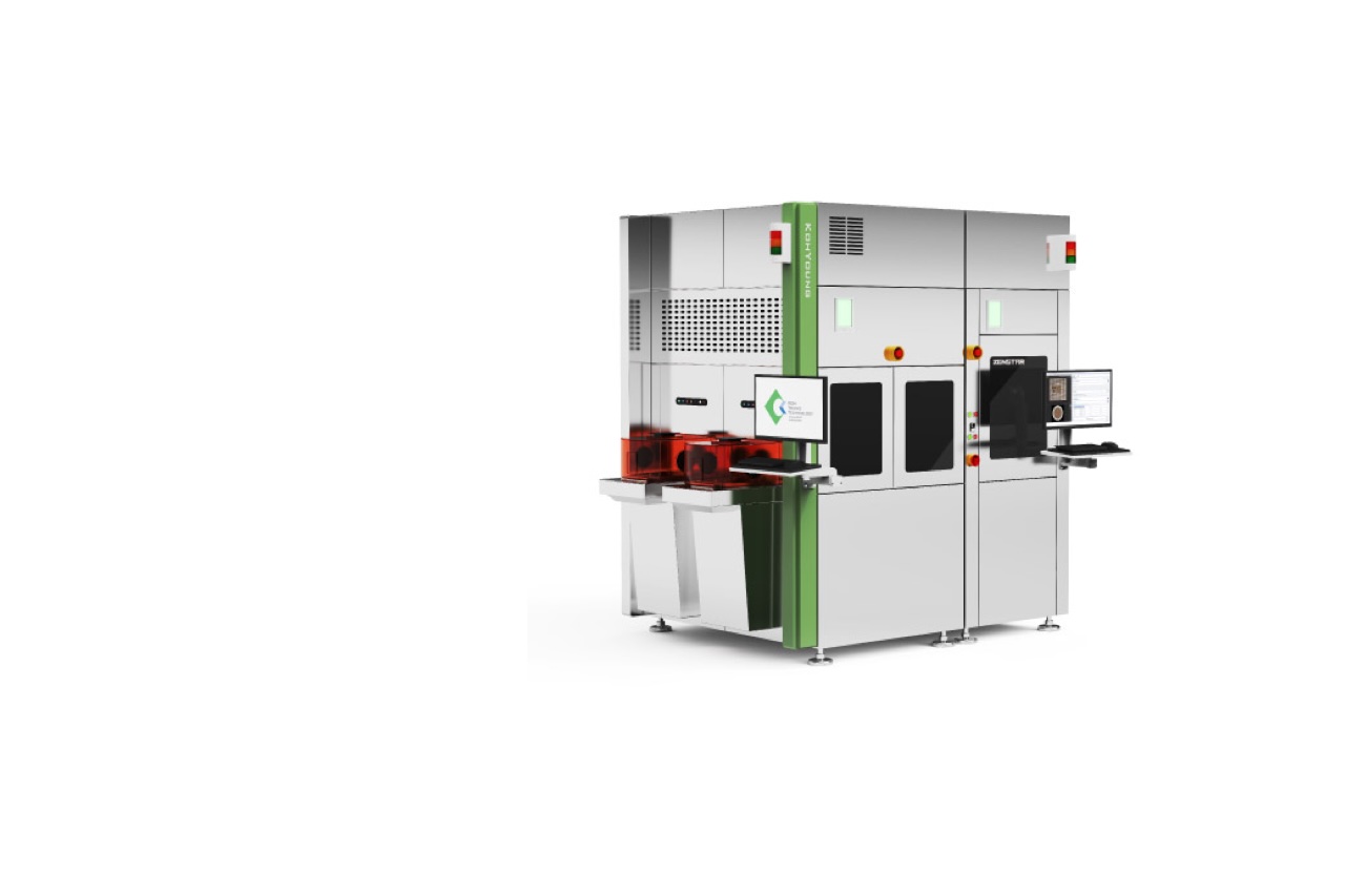
Koh Young will also highlight the continued development of ZenStar, its platform for wafer-level 2D and 3D inspection and metrology. ZenStar extends Koh Young’s measurement technology into increasingly demanding wafer-level applications, including inspection of bumps, pillars, and other micro-scale features. Automated wafer handling options support integration with EFEM and FOUP environments, enabling wafer transfer and inspection within semiconductor workflows.
Continued development of the platform, including the high-resolution Zeta probe, extends Koh Young’s measurement capabilities toward feature sizes beyond the traditional micro-bump range. This provides a path for applying True 3D measurement as wafer-level interconnect dimensions continue to shrink.
Together, the Meister Series and ZenStar allow Koh Young Technology to address inspection requirements ranging from system-level advanced packaging and flip-chip applications to increasingly demanding wafer-level processes.
Addressing a Multi-Platform Advanced Packaging Market
The continued convergence of semiconductor packaging and system-level electronics assembly is creating new requirements for inspection. Advanced packages increasingly combine die, substrates, bumps, pillars, solder, flux, and conventional surface-mount components within the same manufacturing ecosystem. That convergence creates an opportunity for measurement technologies capable of moving with customers across multiple packaging architectures and process stages.
“Advanced packaging is becoming a multi-platform market, and we do not expect one inspection configuration to solve every application,” said Joel Scutchfield, General Manager of Koh Young America. “SiP, flip chip, fan-out, panel-level, and wafer-level processes each bring different measurement challenges. Our approach is to start with the same foundation of accurate 3D measurement and then apply the optics, resolution, algorithms, and handling the application requires. Meister allows us to extend our experience into die, solder, flux, and advanced package inspection, while ZenStar takes that capability further into wafer-level processes. That gives us a path to support customers as packaging architectures and feature sizes continue to evolve.”
The approach also reflects a broader shift in semiconductor manufacturing. Rather than treating inspection as a pass/fail operation at the end of a process, measurement data can provide real-time insight into process variation while there is still an opportunity to correct it. Accurate dimensional information helps engineers maintain tighter process windows, identify emerging trends, improve yield, and reduce the risk of adding value to packages that already contain process-related defects.
At SEMICON West 2026, Koh Young will demonstrate how the Meister S+, Meister D+, and ZenStar address those requirements across multiple stages of advanced packaging manufacturing.
Visit Koh Young in Booth 947 at SEMICON West 2026, October 13–15 at the Moscone Center in San Francisco, to explore how True 3D measurement-based inspection can help address emerging semiconductor and advanced packaging challenges. For more information, visit www.kohyoungamerica.com.
About Koh Young Technology, Inc.
Koh Young helps manufacturers prevent defects, stabilize processes, and increase throughput. Since 2002, the company has led True3D™ measurement-based metrology and inspection, beginning with the industry’s first 3D solder paste inspection system using patented dual-projection Moiré technology. Building on that foundation, Koh Young addresses complex applications including machined parts, press-fit and through-hole pins, conformal coatings, dispensed materials, and semiconductor packaging. A continuous innovation mindset and a customer-focused R&D approach underpin its leadership. With global operations and regional teams, Koh Young provides local support, training, and process expertise that turn inspection data into decisive, closed-loop action for a smarter factory.