Koh Young Technology, the industry leader in True3D™ measurement-based inspection solutions, will participate in the 37th Annual Electronics Packaging Symposium (EPS), September 9-10, 2026, at the Center of Excellence Building within Binghamton University’s Innovative Technologies Complex in New York.
Hosted by the Integrated Electronics Engineering Center (IEEC), GE Research, IBM Research, and CAMM, the two-day symposium brings together leaders from industry, academia, and government to explore the technologies shaping the future of electronics packaging. This year’s program addresses advanced packaging for artificial intelligence, chiplet-based architectures, heterogeneous integration, photonics packaging, advanced substrates, thermal management, and high-performance computing.
As packaging architectures become more complex, inspection and metrology requirements are becoming more diverse. Smaller features, tighter process windows, reflective surfaces, new materials, and increasingly varied package configurations require accurate dimensional data that can help manufacturers characterize processes, identify variation, and improve production decisions.
At EPS, Koh Young will highlight how its measurement technologies and AI-powered inspection capabilities are extending from electronics assembly into semiconductor and advanced packaging applications.
Measurement for a More Complex Packaging Landscape
Koh Young’s advanced packaging portfolio builds on the measurement principles that established the company as a leader in solder paste inspection and automated optical inspection. Rather than relying primarily on image comparison, Koh Young solutions generate quantitative three-dimensional measurement data that manufacturers can use to better understand both product quality and process behavior.
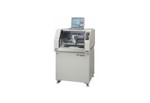
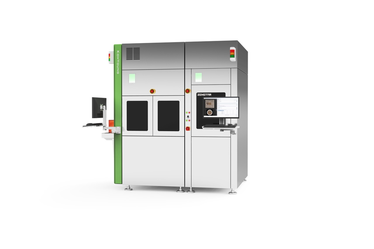
The Meister Series addresses demanding semiconductor and advanced packaging applications, including high-resolution measurement of micro solder deposits, dies, miniature components, narrow gaps, and challenging reflective surfaces. At the wafer level, ZenStar combines True3D measurement with multi-modal inspection and AI-powered vision technologies to evaluate critical package features and identify defects earlier in the manufacturing process.
Together, these platforms help manufacturers capture meaningful measurement data across increasingly complex packaging processes, supporting tighter process control, greater repeatability, and improved yield.
“Advanced packaging is not evolving around one process or architecture. Chiplets, heterogeneous integration, wafer-level packaging, and other emerging technologies are creating different measurement challenges depending on the device, material, and process flow,” said Brent Fischthal, Head of Global Marketing at Koh Young. “That means inspection technology must be both precise and adaptable. Our approach is to provide a strong measurement-based foundation that addresses broad market requirements while giving manufacturers the flexibility to solve the specialized applications that inevitably emerge. EPS gives us an opportunity to discuss those challenges directly with the engineers developing the next generation of packaging.”
Turning Measurement into Manufacturing Intelligence
Koh Young continues to expand the role of inspection beyond defect detection by combining trusted True3D measurement data with artificial intelligence, advanced analytics, and connected software. This approach helps manufacturers identify process variation, improve repeatability, and transform inspection results into information that supports faster and better production decisions.
As advanced packaging moves toward greater density and complexity, understanding how a process is changing can be just as important as identifying an individual defect. Reliable measurement data provides the foundation manufacturers need to optimize processes, protect yield, and address problems earlier.
Koh Young invites EPS attendees to meet with its team during the symposium to discuss advanced packaging applications, emerging measurement challenges, and how True3D metrology and AI-powered inspection can support next-generation semiconductor and electronics manufacturing.
If you cannot join us at EPS, visit Koh Young in Booth 947 at SEMICON West 2026, October 13–15 at the Moscone Center in San Francisco, to explore how True 3D measurement-based inspection can help address emerging semiconductor and advanced packaging challenges.
About Koh Young Technology, Inc.
Koh Young helps manufacturers prevent defects, stabilize processes, and increase throughput. Since 2002, the company has led True3D™ measurement-based metrology and inspection, beginning with the industry’s first 3D solder paste inspection system using patented dual-projection Moiré technology. Building on that foundation, Koh Young addresses complex applications including machined parts, press-fit and through-hole pins, conformal coatings, dispensed materials, and semiconductor packaging. A continuous innovation mindset and a customer-focused R&D approach underpin its leadership. With global operations and regional teams, Koh Young provides local support, training, and process expertise that turn inspection data into decisive, closed-loop action for a smarter factory.