Microscreen, a U.S. manufacturer specializing in high-precision SMT solder stencils and custom tooling solutions, will bring several new capabilities to SMTA International this year, including custom PCB tooling, expanded U.S. manufacturing and new equipment supporting its stencil and screen operations.
The company will exhibit in Booth 3037 at SMTA International 2026, October 27–29 at the Donald E. Stephens Convention Center in Rosemont, Illinois.
One of the biggest additions this year is custom tooling. Through the Microscreen AGI Alliance (MAA), customers now have access to SMT assembly and reflow pallets, screen printer tooling, conformal coating and soldering pallets, router tooling, flying probe, AOI and X-ray fixtures, press-fit tooling and other custom fixtures.
Bringing stencils and tooling together also gives customers the option to source both from one place. The same PCB data can be used to develop the stencil and associated tooling, helping simplify the supply chain while keeping the designs aligned for the application.
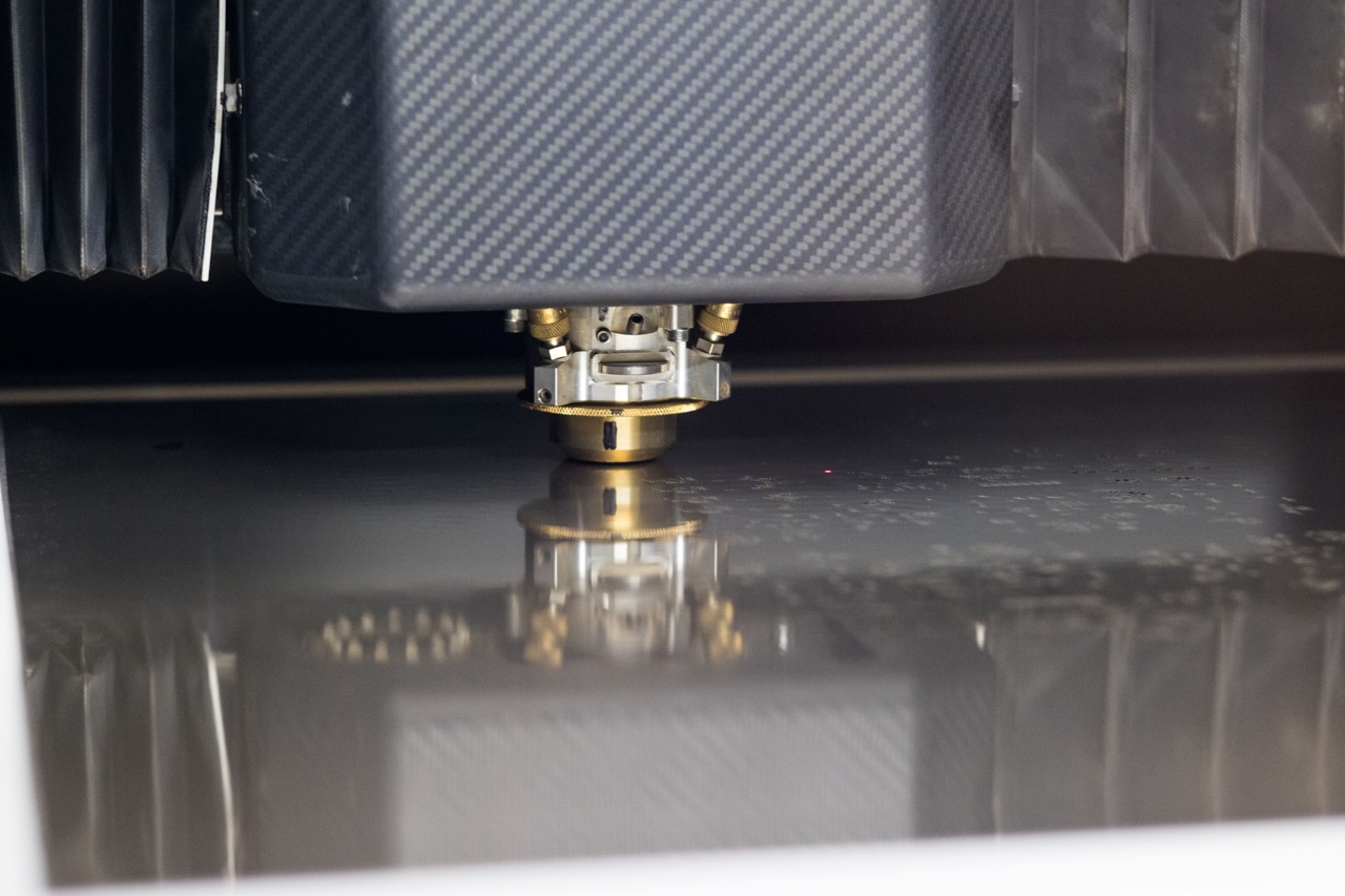
For more than 45 years, stencils and screens have been at the center of what Microscreen does. Today, the company manufactures laser-cut production stencils, step stencils, rework stencils and chemically etched stencils, along with functional metal mesh and polyester mesh screens. Microscreen’s technical staff brings decades of experience in stencil printing and electronics manufacturing, working directly with customers on stencil design, data review and printing challenges.
“We don’t just want someone to send us a file and hope for the best,” said Nik Thomas, Director at Microscreen. “If there’s something we see in the design or a customer is having trouble at the printer, we want to have that conversation. That’s always been a big part of how we do business.”
Microscreen will also feature MicroGlide Platinum, its advanced heat-fused nanocoating designed to reduce paste adhesion and improve solder paste release. The coating is applied to the stencil surface and aperture walls to promote cleaner release and reduce underside cleaning. Microscreen’s original MicroGlide wipe-on nanocoating will also be featured at the show.
Microscreen has also expanded beyond its longtime South Bend, Indiana headquarters with the recent opening of Microscreen CT in Oxford, Connecticut. The new facility adds U.S. manufacturing capacity and provides same day stencil turnaround, with one-day ground shipping available from Maine to Philadelphia.
“As we continue to grow, the personal side of the business is still very important to us,” Thomas added. “SMTA International gives us a chance to sit down with customers, hear what they’re working on and talk through any challenges they’re having.”
Microscreen production stencils are inspected using the Watt SE-12 Pro, following ISO 9001:2015 quality standards.
Attendees are invited to visit Booth 3037 to meet the Microscreen team and learn more about its stencils, screens, nanocoatings and PCB assembly tooling.
About Microscreen
Microscreen is a leading U.S. manufacturer of high-precision SMT solder stencils, step stencils, nano-coated stencils, and custom tooling solutions for the electronics manufacturing industry. For more than three decades, the company has supported aerospace, medical, automotive, industrial, and consumer electronics customers with products engineered to improve print quality, enhance production yield, and support demanding manufacturing environments.