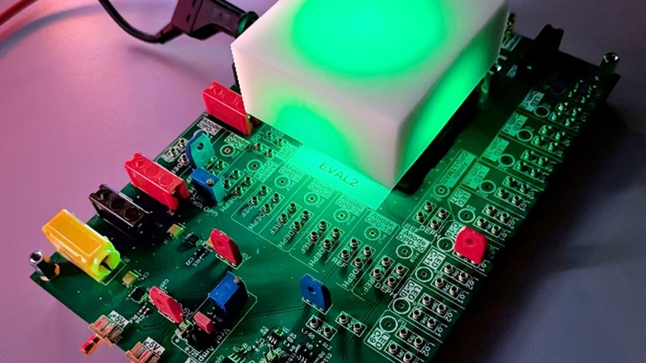
CEA-Leti today demonstrated a co-packaged microLED and organic photodetector (OPD) architecture that enables optical sensing functions. This solution paves the way to integrate sensing capabilities directly within a microLED display, without compromising display performance.
The work, presented in the Photonics West paper, “Co-Packaging of Organic Photodetector with MicroLED Matrix for Multifunctional Display Bio-Application”, validates a system-level approach combining device design, electronics, and modeling for multifunctional display applications.
MicroLEDs deliver high radiance using only a limited fraction of the pixel surface, leaving space for additional functionality. Leveraging this characteristic, CEA-Leti developed a microLED array co-packaged with a tailored OPD, with both devices optimized for operation at green wavelengths relevant to photoplethysmography (PPG) signal extraction.
Technology Performance Assessment
To move beyond component-level demonstrations, the researchers designed a dedicated electronic platform enabling full end-to-end characterization of the complete signal chain—from microLED driving, through a device under test, to photodetection and readout circuitry. Lock-in detection techniques were implemented to improve signal-to-noise ratio and suppress static parasitic components. This is particularly relevant for biosensing detection where AC/DC ratio should be enhanced.
System validation was performed using optical phantoms engineered to replicate the absorption and scattering properties of biological tissue. This approach provided a controlled and repeatable environment for assessing biosensing performance under realistic conditions. Experimental results were combined with analytical modeling to derive a closed-form expression linking microLED operating conditions, photodetector responsivity, and device-under-test reflectance to the detected signal.
The co-packaged microLED devices demonstrated optical power up to 12 mW at a wavelength of 525 nm. On the detection side, OPD responsivity was tuned by adjusting the thickness of the ZnPc active layer to align with the microLED emission peak, achieving a responsivity of 0.083 A/W at the wavelength of interest.
Benefits of MicroLED Technology
The results show that microLED displays can support integrated optical sensing at the pixel level without forcing trade-offs between brightness, resolution, and sensing area. Unlike OLED-based approaches, where display and sensing functions compete for the same surface, this architecture allows both functions to coexist within the same front plane.
The fully characterized, end-to-end system establishes a technical foundation for displays that combine visual output with integrated sensing and adaptive functions, with potential relevance for next-generation displays. Rather than relying on sensors located usually in the bezel of the display, this approach enables sensing capabilities to be designed directly into the display and widespread.
System-Technology Co-Design Approach
“This work illustrates CEA-Leti’s system-technology co-design approach, from concept definition and microLED technology to photodetector co-design, electronics development, and experimental validation under realistic conditions,” said Michaël Pelissier, lead author of the paper. “By combining hardware development with analytical modeling and simulation, we establish a concrete framework for evaluating and scaling sensing-integrated display architectures.”
The study establishes practical know-how for co-integrating microLED displays and optical sensing functions. The architecture is inherently scalable and can be adapted to different pixel pitches and resolutions, depending on the targeted application—from medium-size displays such as smartphones and wearables to larger formats including monitors and televisions.
The results provide a technical foundation for future multifunctional displays in which visual output and sensing capabilities are designed together, at the system level, rather than added as separate components.
This work is part of the IPCEI Microelectronics and Connectivity and was supported by the French Public Authorities within the frame of France 2030.
To learn more, visit www.cea.fr/english.


