
In optoelectronic manufacturing, every micrometer, every millisecond, and every saved process step counts. That is why micrometer adjustment is so important. With the NanoSolder system, nanosystec combines active precision alignment of optical components with selective laser soldering. This enables nanosystec to achieve an ideal combination of precision, reproducible energy input, connection stability, and cost-effectiveness.
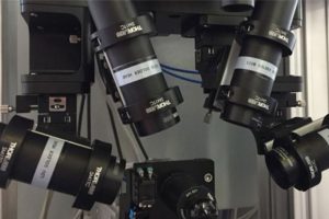 The NanoSolder system enables high-precision positioning of optical components such as integrated photonic circuits, waveguides, diode lasers, and photodiodes. Thanks to precise axis movements in the sub-micrometer range, active alignment ensures optimum coupling efficiency. One focus is the high-precision processing of gold-plated optical fibers. These are first metallized, then solder paste or a suitable preform is applied and melted precisely with a laser beam. The resulting metallic connection is force- and form-fitting and impresses with its high thermal, mechanical, and electromagnetic resilience. The system can also be used on fiber arrays (FAU), in which several fibers are connected to a photonic chip, for example. This requires the appropriate preparation of the components and contact surfaces.
“Compared to adhesive bonds, soldered joints are particularly stable when components are repeatedly exposed to extreme temperature changes or electromagnetic radiation. A typical application can be found in the field of quantum computing,” emphasizes Guenter Hummelt, Managing Director of nanosystec, adding: ” In this case, the chips on which the computing processes run operate at millikelvin temperatures in a Dewar flask. If the chip has to be removed and cooled down again multiple times, this causes considerable thermal stress, which can cause adhesive bonds to become brittle and break, whereas metallic solder joints remain dimensionally stable and resilient.”
The laser is used to melt the solder material in a precise manner. During the soldering process, the temperature profile is stored for tracking purposes. A pyrometer actively regulates the heat input, ensuring precise energy input and process control. This leads to reproducible soldering results. “This targeted energy input means less thermal stress on adjacent sensitive components, less material distortion, and a permanently stable connection, which is a decisive factor, especially in high-quality optoelectronics,” adds Guenter Hummelt.
The combined process of active alignment and selective laser soldering eliminates waiting times for adhesive curing or time-consuming manual readjustments. This leads to a significant reduction in cycle times and an increase in throughput, which directly reduces the cost per unit.
Nanosystec will be presenting its solutions from January 20 to January 22 at booth 3281 at SPIE Photonics West in San Francisco.
About nanosystec:
nanosystec GmbH develops and manufactures high-precision assembly and testing systems for industrial series production. Based in Gross-Umstadt near Darmstadt, the company has been a partner to leading manufacturers in optoelectronics, medical technology, the automotive industry, and aerospace since 2001. The systems are based on finely tuned motion control and integrate processes such as precision laser welding, UV micro-bonding, and fine balancing. Thanks to modular platform architecture and high repeatability in the sub micrometer range, both highly flexible and cycle time-optimized production solutions can be realized. In addition to standard modules, nanosystec also offers customized complete solutions including process development, integration, and lifecycle support.


