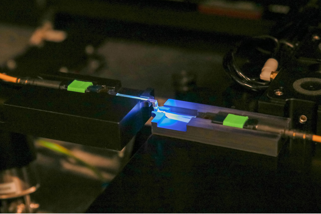
Photonics is a key technology for the 21st century and is the basis for ultra-fast data transmission, high-precision sensor technology, and cutting-edge communication and computing technologies. To ensure that Europe remains technologically independent in these strategically important areas, it needs specialized solution providers who can manufacture complex optoelectronic assemblies with the highest precision. Tresky Automation is playing a central role in developing high-performance machine platforms Made in Germany for the microelectronics packaging and connection technology of photonics and optoelectronics systems.
‘Our machines are not only precise, but they also think ahead,’ says Daniel Schultze, Managing Director of Tresky GmbH, adding: ‘Active alignment means real-time correction, optical feedback and maximum yield. Once you’ve worked with it, you’ll never want to go back.’
Such modern photonics solutions have become indispensable in safety-critical systems. Fiber-optic-based communication builds the backbone of modern IT infrastructures and enables encrypted data connections in civil, industrial and military environments. LiDAR systems in autonomous vehicles capture the environment with the highest accuracy, while optical transceivers in satellites create the basis for fast and interference-resistant data connections. Photonics is also an indispensable element for new applications in aerospace, medical technology and quantum technology. Optical sensor technology, laser-based distance measurement, infrared-supported threat detection and optical neural networks for AI-controlled systems not only require the highest technological standards, but also absolutely reliable manufacturing processes.
Active alignment technology plays a key role in these processes. In contrast to passive alignment, where components are positioned based on geometric features, active alignment relies on signal feedback during assembly. This ensures that not only the geometric center is achieved, but also the actual maximum performance of the light coupling. This precision is particularly crucial in applications with single-mode fibers or in silicon photonics systems, where even the smallest deviations can lead to significant losses. Hybrid modules with multiple optical interfaces and non-standardized geometry also benefit from this active alignment strategy. Tresky combines nanometer accuracy with flexible assembly methods in various coupling processes.
Edge coupling is a coupling method in which light is fed directly into the laterally exposed waveguide of a chip. The optical connection is made via the cleaved facet, i.e. a polished or cut edge of the photonic component. This method enables particularly low-loss couplings, typically with a coupling efficiency of less than 1 dB, and is therefore ideal for demanding high-performance applications such as silicon photonics (SiPh), laser modules or high-speed optical connections. Since edge coupling requires extremely precise adjustments, especially when using single-mode or polarization-maintaining fibers, only active alignment is used here. Only continuous evaluation of the optical signal in combination with high-resolution positioning movements can compensate for the unavoidable tolerances of the components. This coupling of signal evaluation and precision positioning enables the optical signal to be maximized, resulting in reliable construction in the nanometer range.
Another process is grating coupling, also known as surface coupling. This is an established method of optical coupling in which light is coupled into the waveguide of a chip vertically rather than laterally via surface-structured grids. The light is usually guided by fibers that are directed at the grating at a defined angle, typically between six and ten degrees. This coupling approach allows for greater tolerances in vertical alignment (Z-direction) and is therefore particularly well suited for wafer-level testing or compact optoelectronic modules where space and flexibility are crucial. Although the coupling efficiency is slightly lower than that of edge coupling, with a loss of around 3–5 dB, grating coupling offers decisive advantages in process integration due to its comparatively simple handling and adjustability, especially in the characterization of photonic chips or in the construction of modular sensor units. In automated manufacturing processes, the method can be efficiently combined with active alignment to ensure stable and reproducible light paths.
Other coupling methods include lensed fiber, lens coupling and free-space coupling. These methods enable an optical connection between components without direct physical contact. They are primarily used when classic coupling methods such as edge or grating coupling reach their limits. The light is focused using special lenses, such as spherical, cylindrical or aspherical micro-optics, in order to transmit it with low loss across an air gap into the waveguide or onto the optical target. Lensed fibers, in which the lens is integrated directly into the fiber, or external lens systems, which allow additional degrees of freedom in adjustment, are frequently used. This type of coupling is characterized by high flexibility and mechanical decoupling. Since there is no direct contact between the fiber and the chip, applications with special requirements in terms of cleanliness, vacuum compatibility or long-term stability can also be implemented, for example in space travel, high-power laser modules or hybrid opto-mechanical structures. In addition, the process offers the possibility of precisely optimizing the beam path through active alignment with angle and distance correction. This is particularly advantageous for complex, multi-channel or non-standard geometries.
Free-space coupling, by contrast, places high demands on the optomechanical stability of the system, as even the smallest positional changes can lead to adjustment losses. With suitable machine technology, such as that provided by Tresky Automation, it is possible to achieve precise and reproducible coupling. This makes the process ideal for exceptionally demanding applications in research, defense, medical technology, and quantum optics.
Loop coupling is used to control and distribute optical signals within waveguide-based systems. Light is guided through a closed optical structure, often a microring or microloop, in which part of the light is coupled between adjacent waveguides. This allows precise control of resonance behavior, wavelength filtering, and signal modulation. In photonics applications, loop coupling plays an important role in the implementation of compact optical filters, wavelength division multiplexers (WDM), and sensors. By specifically adjusting the coupling degree and loop geometry, bandwidth, quality factor, and sensitivity can be precisely set. Loop coupling thus enables high-density, low-loss, and adaptable photonic integrations. This represents a key component of modern communication, LiDAR, and sensor systems.
In fiber coupling, also known as direct coupling, the light generated by a light source, such as a laser diode or a VCSEL, is precisely coupled into an optical fiber. This connection is one of the central interfaces in photonics, as it enables the efficient transmission of light signals between components, modules, or systems. Precise alignment, positioning accuracy in the nanometer range, and the thermal and mechanical stability of the connection are crucial for high coupling efficiency. Modern active alignment technologies and precise bonding systems ensure that power losses are minimized, and long-term stability is guaranteed. Fiber coupling is used in areas such as telecommunications, sensor technology, medical diagnostics, LiDAR systems, and photonics packaging.
Array coupling refers to the precise optical coupling of multiple light sources or waveguides in photonic systems. This technology plays a key role in modern photonics applications, such as the coupling of laser arrays, VCSELs, or fiber bundles to photonic integrated circuits (PICs). The goal is to connect multiple channels simultaneously with minimal loss and high positioning accuracy <1 µm. This is achieved using high-precision adjustment methods, active alignment technologies, and special lens arrays or grating couplers. Array coupling thus enables efficient data transmission in high-speed communication, sensor technology, LIDAR, and quantum photonics—anywhere where compact, scalable, and low-loss optical interfaces are required.
Tresky Automation’s machine platforms are designed to cover the entire process, from precise component positioning and optical alignment to final bonding. Customer-specific requirements as well as future scalability are both taken into account. The modular architecture allows the integration of a wide range of process steps, such as bonding, curing, optical and electrical pre-testing, and automated assembly of fibers, lenses and laser diodes. The combination of high flexibility and process reliability results in manufacturing solutions that are suitable for both research and development as well as series production.
‘’However, we go one step further. Our DIE bonders combine all relevant bonding technologies in a single system, including thermocompression bonding (TCB), adhesive bonding, ultrasonic bonding, sintering and flip-chip bonding. These universal platforms make Tresky systems unique on the market and offer maximum flexibility without compromising on precision or process reliability,” Schultze continues. “With this innovation, Tresky GmbH emphasizes its role as a technology leader in the field of DIE bonding and offers a solution that meets the increasing demands of the photonics industry, from prototype production to industrial scaling.”
At productronica/SEMICON Europe, which will take place from 18 to 21 November at the exhibition center in Munich, Tresky will be presenting not only Active Alignment but also all other DIE bonding processes at booth 321 in hall B2.
About Tresky
Since 2013, the name TRESKY Automation has stood for the highest quality, flexibility and maximum reliability. As one of the world’s leading machine manufacturers for placement systems in the high-precision sector, Tresky GmbH specializes in the development and production of innovative bonding solutions.
The philosophy of Tresky Automation is based on the principle of quality “Made in Germany”. This means that all development, production and sales processes take place at the headquarters. Tresky GmbH is based in Hennigsdorf, a town close to the capital Berlin. This location is not only strategically favorable, but also of great importance, as it is home to numerous highly specialized companies from the automation, electrical and communication technology and life science sectors.
Tresky – DIE Bonder for R&D and Production


