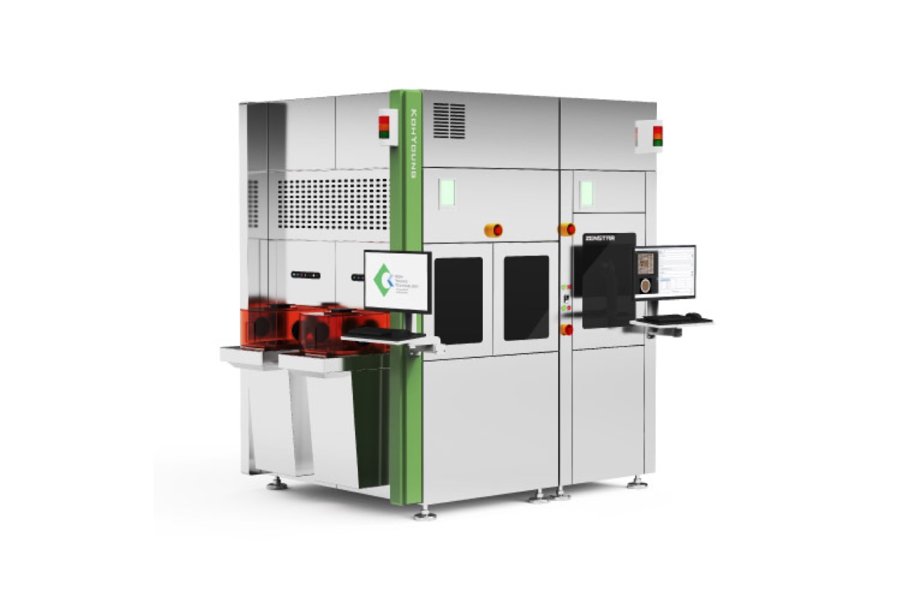
Koh Young, the industry leader in True 3D measurement-based inspection and metrology solutions, will showcase its Meister D+ and ZenStar systems at SEMICON Europa 2026, taking place 10–13 November at Messe München, Germany. Visitors to Booth C2.329 can explore how these complementary platforms address demanding inspection requirements in advanced packaging and wafer-level manufacturing.
As semiconductor packages become more complex, smaller features, tighter spacing, and highly reflective surfaces create new challenges for inspection and process control. Koh Young combines accurate, repeatable 3D measurement with specialized optics and application-specific algorithms to help manufacturers detect defects, understand process variation, and improve yield.
Exhibition Highlights
With the Meister D+ on display, Koh Young will demonstrate how True 3D measurement addresses key inspection challenges across advanced packaging and wafer-level manufacturing, including:
- Reflective Die Inspection: True 3D measurement of highly reflective and mirror-finish die surfaces supports reliable evaluation of die height, tilt, coplanarity, and position.
- High-Density Packaging: Inspection of small die and narrow gaps helps manufacturers address increasingly compact package designs and tighter dimensional tolerances.
- Wafer-Level Metrology: Combined 2D and 3D inspection provides detailed information on bumps, pillars, and other micro-scale features.
- Actionable Measurement Data: Objective dimensional information helps engineers identify emerging variation and optimize processes before defects affect subsequent manufacturing stages.
Meister D+ Advanced Die Inspection and Metrology
The Meister D+ combines Koh Young’s Moiré measurement technology with proprietary optics engineered for highly reflective die and complex package features. The system measures critical placement characteristics while detecting defects such as micro-cracks, chipping, and foreign material. Supporting small die and narrow-gap inspection down to 50 µm, the Meister D+ addresses high-density packaging applications where conventional optical techniques can struggle. Its dimensional measurement data helps engineers assess placement quality and identify variations that can compromise package integrity.
ZenStar Wafer-Level 2D and 3D Inspection
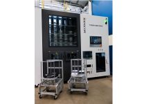
ZenStar extends Koh Young’s measurement capabilities into wafer-level inspection and metrology, including bumps, pillars, and other micro-scale structures. The platform combines 2D and 3D inspection to address the evolving requirements of wafer-level packaging and increasingly fine interconnect features. Automated wafer handling options support integration with equipment front-end modules (EFEM) and front-opening unified pod (FOUP) environments, enabling wafer transfer and inspection within semiconductor manufacturing workflows.
Visit Koh Young
See the Meister D+ and ZenStar on the exhibition floor and meet Koh Young Europe’s team to discuss your advanced packaging and wafer-level inspection requirements.
Visit Booth C2.329 at SEMICON Europa 2026, 10–13 November at Messe München, Germany.
About Koh Young Technology, Inc.
Koh Young helps manufacturers prevent defects, stabilize processes, and increase throughput. Since 2002, the company has led True3D™ measurement-based metrology and inspection, beginning with the industry’s first 3D solder paste inspection system using patented dual-projection Moiré technology. Building on that foundation, Koh Young addresses complex applications including machined parts, press-fit and through-hole pins, conformal coatings, dispensed materials, and semiconductor packaging. A continuous innovation mindset and a customer-focused R&D approach underpin its leadership. With global operations and regional teams, Koh Young provides local support, training, and process expertise that turn inspection data into decisive, closed-loop action for a smarter factory.