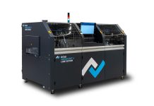
The rapid development of artificial intelligence is driving the demand for high-performance processors and placing great demands on electronics manufacturing. As the world’s leading provider of hardware and software for semiconductor and electronics production, ASMPT is meeting these challenges with innovative placement technology that is capable of processing both super-miniaturized components and large, heavy AI chips with exceptional precision. With automated measurements, intelligent vision systems and adaptive placement mechanisms, SIPLACE placement platforms deliver error-free assembly processes – even for components with thousands of contacts arranged in complex patterns.
Processors – the heart and brain of server boards, are becoming ever larger and more powerful. Over the last three years, the size of processors has grown at an unprecedented pace as a result of the exponentially rising need for computing performance that has been triggered primarily by the rapid development of artificial intelligence and its enormous data processing requirements.
“Modern electronic products place extreme demand on the assembly technology,” explains Thomas Bliem, Vice President R&D at ASMPT SMT Solutions. “Large AI chips with ball grid arrays and highly miniaturized standard components that are placed in the tightest spaces must be placed with great precision. All these very different components must be processed on a single line, and as closely as possible to the ideal of zero defects per million opportunities (DMPO). This is an area where ASMPT is leading as a technology pioneer. With our trendsetting machines, electronics manufacturers are ready for the future.”
Smallest components in the tightest of spaces
Modern 0201m components are smaller in width than a human hair and get placed with extremely tight pitches. As a result, their housing can no longer self-center during the reflow process, so that even the smallest misalignment leads to a short circuit, making the whole product unusable. SIPLACE placement machines measure each component individually and use their rotating head segments to compensate for any pickup offsets. Each segment can be rotated individually. After the component has been picked up, it is brought to the placement position on its way to the camera, for example at an angle of 90°. After the optical measurement, only a minimal angle correction is required, which is usually less than 1°. This unique principle in the SIPLACE placement machines not only achieves the highest placement accuracy, but also allows any placement angle, such as 35°, to be realised.
Large and heavy BGA chips
Modern AI applications require a lot of computing power, which means that processors are becoming ever larger and more complex. Most of them are built as system-in-package (SiP) components containing bare dies as well as passive standard SMT components. Some of them already measure 80 × 80 mm and weight more than 100 grams, with form factors of 150 × 150 mm and weights of 300 grams being predicted for the near future. The SiP design also means that the center of gravity of these processors is not always the same as their physical center, which is why SIPLACE placement machines must determine the inertia of these heavy ball grid arrays (BGAs) with precisely defined rotational movements. This allows them to ensure that the component is moved with the maximum possible acceleration without inertia-related disturbances.
Soon: 10,000 to 20,000 connections
Modern AI processors require huge numbers of contacts that will soon be in the tens of thousands. Since they are also spread irregularly across the connecting surface, describing them manually would take forever. Using their component camera, SIPLACE placement machines can read contacts automatically or import the manufacturer’s geometrical data via a standardized interface. Needless to say, this also applies to the SIPLACE Vision Teach Station. And to safely pick up these BGAs, ASMPT offers a broad portfolio of individually shaped nozzles.
Optical inspection of components
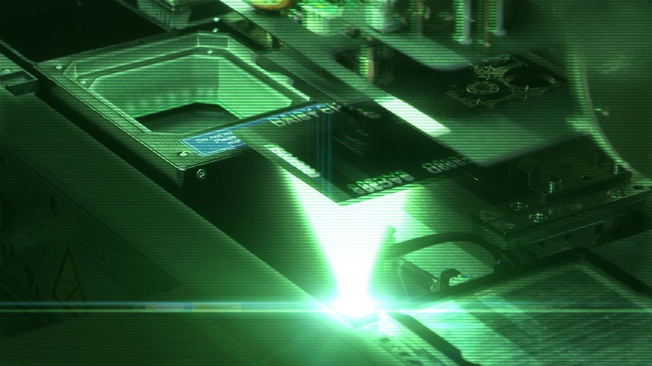
Inspecting large BGAs optically with the component camera is crucial for a successful placement process. The system checks, for example, whether pin 1 is in the right position and whether all solder balls are present. Equally important is the high-precision coplanarity test. Only if all balls lie exactly on the same plane can they make proper contact with the solder paste deposits, which are only 100 microns thick. Since the accuracy of the component camera is insufficient for this measurement, SIPLACE placement machines operate with a coplanarity module that projects a laser beam onto the connection level. By moving the component relative to the laser beam while scanning it, the machine employs a special algorithm to determine a precise 3D height profile.
PCB inspection
SIPLACE placement machines inspect the placement position on the PCB with another high-resolution vision system, the PCB camera. It is used to detect and examine things like spacer components, which are essential for a trouble-free reflow process as they prevent short circuits caused by the inevitable thermal twisting of large BGAs. The PCB camera also detects any foreign objects in the placement area.
AI components are too expensive for faulty placements
Only when all measuring systems have given their OK, when all solder balls are on the same plane and any Z-deviations are within the tolerance range and the target area on the circuit board meets all the requirements will the BGA be placed with maximum precision and a precisely defined force. This effort is worth it because the price of state-of-the-art AI processors can be very high.
About ASMPT Limited (“ASMPT”)
ASMPT Limited is a leading global supplier of hardware and software solutions for the manufacture of semiconductors and electronics. Headquartered in Singapore, ASMPT’s offerings encompass the semiconductor assembly & packaging, and SMT (surface mount technology) industries, ranging from wafer deposition to the various solutions that organize, assemble and package delicate electronic components into a vast range of end-user devices, which include electronics, mobile communications, computing, automotive, industrial and LED (displays). ASMPT partners with customers very closely, with continuous investments in R&D helping to provide cost-effective, industry-shaping solutions that achieve higher productivity, greater reliability, and enhanced quality. ASMPT is a founding member of the Semiconductor Climate Consortium.
To learn more about ASMPT, please visit www.asmpt.com


