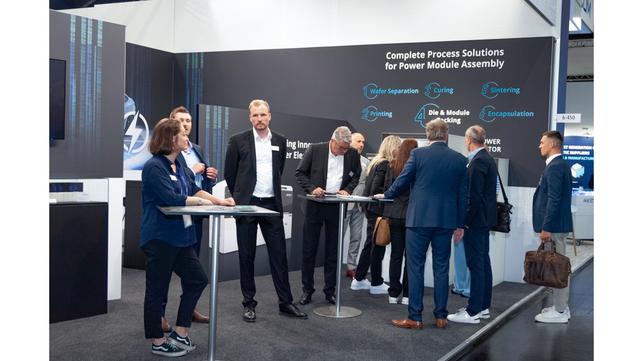
At the PCIM Europe industry fair in Nuremberg, ASMPT exhibited a complete power module manufacturing concept. With its presentation of innovative laser dicing and sintering technologies, the global market and technology leader in hardware and software solutions for semiconductor and electronics production addresses current challenges in the production of power electronics for the automobile industry and beyond.
“Against the backdrop of recent supply chain challenges, the European automobile electronics industry has a great interest in having more chips and components manufactured in Europe. Power electronics in particular are developing great momentum, as was apparent at the PCIM show,” says Johann Weinhändler, Managing Director at ASMPT AMICRA GmbH in Regensburg, who is responsible for ASMPT’s Semiconductor Solutions segment in EMEA in addition to the global AMICRA business. “With our help, European EMS providers will conquer new business areas.”
David Felicetti, Business Development & Product Marketing Manager at ASMPT, added: “With their high efficiency and thermal conductivity, power modules that are based on silicon carbide (SiC) and firmly bonded to heat sinks via silver sintering are increasingly in demand for automotive electronics, but other application areas will play a significant role in the future as well. Accordingly, many PCIM visitors showed great interest in our POWER VECTOR die and module bonding platform.” Weinhändler adds: ”We can now offer machines for the complete process chain in power module production. This does not mean, however, that these machines must be arranged in a line, as in our model. I can well imagine that some EMS providers will specialize in process steps such as sintering.”
As part of its sustainability strategy, ASMPT refrained from shipping giant machines to Nuremberg and instead presented its machines as mock-ups and models in combination with 3D videos.
In addition to the process chain for power modules, the presentation of the ALSI LASER1205 multi-beam laser dicing platform sent another important message: With its patented new process, it improves the yield in the separation of thin, sensitive and still very expensive SiC wafers. The innovative system processes wafers ranging from 10 to 250 microns in thickness with a positioning accuracy of less than 1.5 microns, and it operates 50 percent faster than conventional methods.
To learn more about ASMPT, please visit www.asmpt.com.


