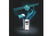
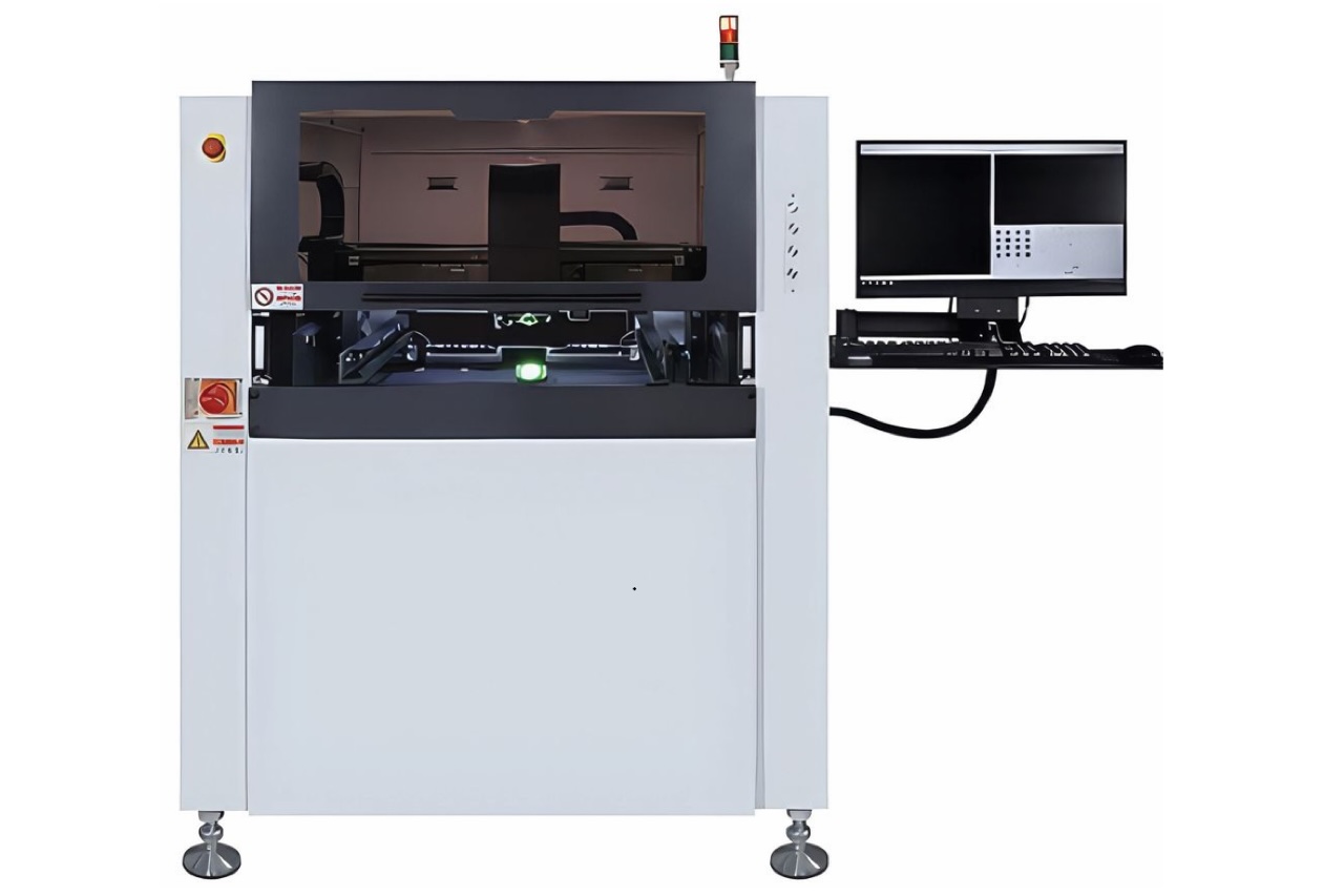
Seika Machinery, Inc., a leading provider of advanced machinery, materials and engineering services, announces that its Sawa T100 Automatic Stencil Inspection System has been selected as the core stencil metrology platform for the Ultra-High-Density Interconnect (UHDI) Consortium, an industry-collaborative research initiative conducted at Rochester Institute of Technology (RIT).
Organized and managed by 360 Circuits under the guidance of an industry advisory board, the UHDI Consortium is designed to advance the understanding of solder paste printing technologies for next-generation high-density electronics assembly. The research brings together industry suppliers, technical experts and academic researchers to evaluate stencil technologies under controlled, independent testing conditions.
The Sawa T100, supplied by Seika Machinery, has been installed and is operational at the SMTA Laboratory at RIT, where it plays a central role in evaluating stencil quality, aperture geometry and measurement repeatability. A primary objective of the consortium is to validate the T100 as a reliable measurement reference for increasingly demanding UHDI printing applications.
As electronic assemblies continue to incorporate smaller components, finer features and thinner stencil foils, accurate stencil inspection becomes increasingly important to maintaining solder paste deposition consistency and manufacturing yield. The consortium addresses these challenges through a double-blind testing protocol that evaluates stencils from multiple suppliers using common test vehicles and standardized measurement procedures.
The study encompasses laser-cut, electroformed, nickel and nanocoated stencil constructions across a range of foil thicknesses, providing comparative data on technologies from North American, Asian and European suppliers. Results will contribute to peer-reviewed technical publications and support continued research into fine-feature SMT printing.
At the center of this effort, the Sawa T100 provides automated aperture metrology, measuring aperture dimensions and positions against Gerber design data across the stencil field. The system also incorporates an integrated tension gauge to evaluate stencil mesh tension at multiple locations, supporting consistent inspection and delivery-acceptance procedures.
Engineered for high-precision measurement, the T100 features a thermally stable, zero-level marble base, linear-motor motion with closed-loop positioning, high-resolution optical inspection and automated programming directly from Gerber data. Additional capabilities include statistical process control (SPC) reporting, manufacturing execution system (MES) connectivity and stencil management functionality.
“Participation in the UHDI Consortium provides an important opportunity to demonstrate how advanced stencil inspection can support the industry’s transition toward increasingly fine-feature electronics assembly,” said Michelle Ogihara, EVP. “By contributing the Sawa T100 to this independent research program, we are supporting the development of repeatable measurement methods that can help manufacturers better understand stencil quality and improve process control.”
The consortium’s research program consists of three phases, beginning with baseline process development and validation of the T100 measurement methodology. Subsequent phases will evaluate UHDI test vehicles incorporating smaller components, thinner stencil foils and fine-particle solder pastes, followed by reflow studies examining the relationship between solder printing and completed solder joints.
In addition to Seika Machinery and Sawa, participating companies include AIM Solder, MicroScreen, StenTech and Metal Etch. The advisory board includes recognized industry specialists in stencil technology, process engineering, materials and electronics manufacturing research.
As part of Seika Machinery’s commitment to supporting industry education and technology evaluation, the Sawa T100 is available for live demonstrations at RIT by appointment. Electronics manufacturers, process engineers and stencil suppliers interested in seeing the system’s inspection and measurement capabilities firsthand are encouraged to arrange a demonstration.
About Seika Machinery, Inc.
Seika Machinery, Inc. (SMI) is a subsidiary of Seika Corporation, Japan and member of the Mitsubishi Global Group. SMI provides electronics manufacturers with advanced machinery, superior materials and engineering services.